Huawei can't shrink its chips, so it decided to fold them
For fifty years, progress in semiconductors has had a single direction: downward. Smaller transistors, denser, more of them on the same surface. Moore's law was never a physical law but an economic forecast that the industry turned into a collective commitment, building factories, supply chains and an entire competitive order on top of it.
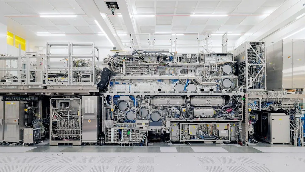
Whoever controls the machines capable of drawing the finest geometries controls the frontier. That is exactly why the export restrictions on ASML's EUV equipment have become the most effective geopolitical tool of recent years: they do not stop China from making chips, they stop it from making those chips.
Huawei responded in a way worth watching, regardless of how much of it actually holds up: instead of chasing the same road with worse tools, it changed the direction of travel.
What it announced
The company presented LogicFolding, an architecture that arranges logic across multiple stacked layers rather than on a single plane. The claimed figures point to 55% more transistor density and 41% better energy efficiency compared with the two-dimensional equivalent.
The commercial debut is planned for the Kirin processors in autumn 2026, extending to the Ascend AI chips by 2030. The stated goal is to reach, by 2031, a density equivalent to a 1.4-nanometer process, without owning a single EUV machine. The 2026 Kirin is quoted at 238 million transistors per square millimeter, a value comparable to TSMC's 3nm.
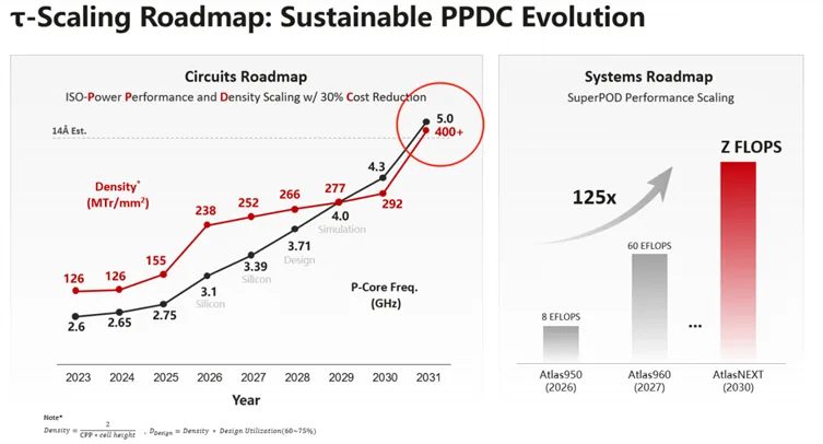
Huawei paired the announcement with a move more significant than the numbers: it proposed its own metric of progress, the Tau Scaling Law, explicitly designed to replace Moore's law as the industry's unit of measure.
This is not a marketing detail. Whoever defines the yardstick by which progress is measured also decides who is winning.
How layered construction works
The core idea is intuitive. If you can't widen the house, build another floor.
In traditional design, the transistors all sit on the same layer of silicon, and the way to have more of them is to draw them smaller. That is exactly what EUV lithography is for, the one step that is off-limits to China. Layered construction sidesteps the problem: it keeps transistors at sizes achievable with the available machines, but arranges them on stacked layers connected vertically.
Here, though, a technical distinction is needed to explain why the matter is harder than it sounds.
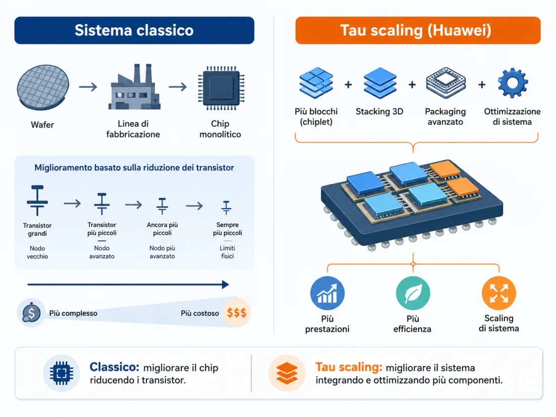
Stacking by bonding is already widespread and has nothing exotic about it. Separate dies are produced and joined together, as happens in the HBM memory that feeds every AI accelerator, or in AMD's 3D V-Cache. The vertical connections, however, are on the order of a micrometer, relatively sparse, and the alignment between layers is coarse.
Monolithic integration is another thing entirely. The layers are not bonded: they are built in sequence, one on top of the other, during fabrication itself. The result is a vertical connection density between 10 and 100 times higher, much smaller distances between layers, and alignment at the nanometer scale. It is the difference between stacking two finished buildings and constructing a tower with the internal staircases in the right place.
It is in this second family that Huawei's approach sits, and from here come the two problems the company itself admits. Heat, because stacking active logic means concentrating dissipated power in a smaller volume, and the inner layers are the hardest to cool. And design complexity, because existing design tools reason in two dimensions. Not by chance, Peking University developed an EDA tool specific to LogicFolding: without software able to think in three dimensions, the architecture stays on paper.
It is not a new technique. It is a different choice
Here something has to be said that many commentaries overlook, and that makes the story more interesting, not less.
Huawei did not invent 3D. Monolithic integration has been studied in the West for twenty years, TSMC has its SoIC, Intel has Foveros, and the academic research on the subject is largely American and European. The technology is known to everyone.
The difference lies not in the knowledge but in the priority.
For a company that has EUV machines, the third dimension is a complement: you keep shrinking, and you stack where it pays off. Nobody bets their roadmap on a riskier technology while the main road still works. It would be irrational, and it would be punished by the market at the first weak quarter.
For a company that does not have the machines, the third dimension is not a complement: it is the only direction left. And when a technology becomes the only road, it receives all the resources, all the brains and all the tolerance for failure that would normally never be granted to it.
The constraint, in other words, did not make Huawei smarter. It made it free to bet everything on a hypothesis that no competitor had any reason to take seriously.
The same logic applied to artificial intelligence
The reasoning is not limited to fabrication. The same pattern shows up in the Ascend 950PR accelerator, produced by SMIC on a 7nm process and in mass production since March 2026: 1 PFLOPS in FP8, 1.56 PFLOPS in FP4, 112 GB of proprietary HiBL memory with 1.4 TB/s of bandwidth, and claimed performance around 2.8 times that of Nvidia's H20 in FP4.
A 7nm chip competing with a product built on more advanced processes is no miracle: it is, once again, the choice to optimize what you can control, memory, bandwidth, numeric formats and architecture, instead of lamenting what is missing.
Even more telling is the software strategy. Nvidia's real moat is not the silicon, it is CUDA: twenty years of libraries, tools and developer habits. Huawei did not try to convince the world to adopt a new language, nor did it settle for a runtime translation layer. With CANN Next it recreated CUDA's fundamental constructs, thread blocks, warps, kernel launches, mapping them directly onto Ascend hardware.
It is a clear reading of reality: CUDA is not a product to beat, it has become a language. And languages are not defeated, they are spoken.
The market is responding. ByteDance has committed more than 5.6 billion dollars to Ascend purchases for 2026, roughly half of the planned annual production of 750,000 units, and DeepSeek V4 runs on this platform. Huawei is aiming for around 12 billion dollars in revenue from AI chips in 2026, against 7.5 billion the year before.
What the West struggles to do
It would be convenient to dismiss all of this as industrial propaganda. It would also be a mistake, because the interesting point is not technical but cultural.
Western industry is not less creative. It is more invested. Decades of capital, factories, expertise and careers are built on the assumption that progress means smaller geometries. That assumption worked beautifully, and for exactly that reason it became invisible: nobody debates it anymore, the way nobody debates gravity.
The result is a system of incentives that makes doubt uneconomical. An executive proposing to move half the budget onto an unproven three-dimensional architecture would be measured on next quarter's results, not on those of 2031. A fund financing an eight-year bet would have to explain to its investors why it did not put the same money where the return is certain.
It is not a lack of intelligence. It is path dependence: when the road you built works, every detour has an immediate cost and a remote, uncertain benefit. So you keep travelling it, faster and faster, in ever greater haste, without ever asking whether it still leads where you need to go.
Whoever does not have that road does not pay the cost of the detour. They only have to invent one.
There is a lesson here, and it is not about semiconductors. It is about the habit of treating the current arrangement as final, and of mistaking for laws of nature what are only very successful conventions. Moore's law was never a law. It was a forecast we found it convenient to turn into destiny.
What remains to be proven
Having said all this, caution is in order, for two reasons.
The first is that the numbers are Huawei's. There are no independent verifications, no third-party benchmarks, no public data on production yields, which in microelectronics are the variable that separates an announcement from a product. An architecture can work in the lab and remain economically unsustainable in the factory.
The second is that equivalent density does not mean an equivalent process. Achieving the transistor density of a 1.4nm process by stacking layers does not automatically solve the problems of power consumption, thermal dissipation and switching speed that a real 1.4nm would face differently. These are results that are comparable on one parameter, not equivalent on all of them.
The fact remains that 381 chip models are already in mass production with related techniques, and that six years of restrictions have not stopped the company they were meant to stop.
What to take away
For anyone who deals with technology inside a company, rather than geopolitics, the practical lesson is closer than it seems.
The architectures we take for granted are almost always the result of historical constraints, not technical truths. The server that has always been there, the supplier that has always been used, the way that process has always been done: none of these things is a law of nature. They are decisions made once, in a context that has since changed, and never questioned again because questioning them costs today and pays off tomorrow.
The useful question is not which technology is best on the market. It is which problem we keep solving the way we have always solved it, simply because nobody ever asked whether there was another direction.
Sources: TechSpot · Tom's Hardware · Tom's Hardware, 3D EDA tool · Elettronica News, Ascend 950PR · SemiWiki